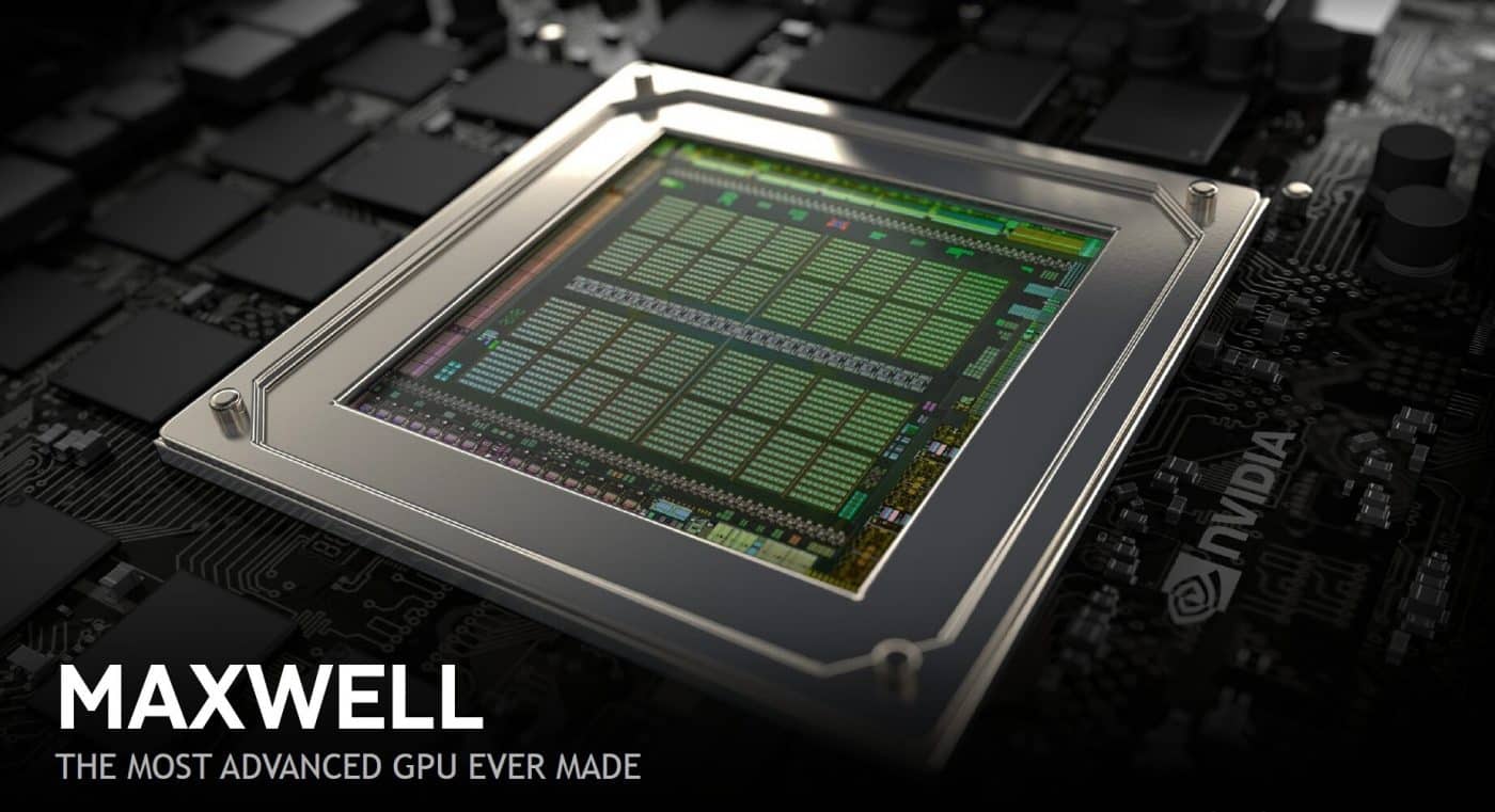
It looks like NVIDIA will not be waiting for the 20 nm fab process for its next big GPU. Riding on the success of the GM204 silicon, the next enthusiast-segment GM200 silicon will be based on the 28 nm silicon fab process. NVIDIA’s GeForce GTX Titan II could be based off this silicon.

A very curious data entry was submitted by an anonymous source to SiSoftware’s hardware database, which gives away the details on the GM200. So as we said the GM200 will be built on the existing 28 nm node and will have a die area of 551 mm2. The chip will be based on the Maxwell architecture and will have 3072 CUDA cores and 3 MB L3 cache.

The chip will most likely have a 384-bit GDDR5 memory interface along with lossless texture compression algorithms which work to step up memory bandwidth. The standard memory amount is 12 GB, which is double that of the first-generation GeForce GTX Titan. The chip will also feature a core clock of 1100 MHz and a boost all the way up to 1390 MHz. The memory is set at 6.00 GHz (effective).
Source: Expreview | News Archive