
AMD’s upcoming Zen 6 processors are poised to deliver a significant leap in performance and efficiency, reportedly utilizing TSMC’s cutting-edge 2nm (N2P) process for core chiplets (CCDs) and 3nm (N3P) for the I/O Dies (IODs). This strategic move, expected around late 2026 or early 2027, marks a substantial advancement from the current Zen 5 architecture.
Key Takeaways
- Advanced Process Nodes: Zen 6 CCDs will be fabricated on TSMC’s 2nm N2P node, while IODs will use the 3nm N3P node.
- Performance Boost: Expect higher clock speeds, potentially reaching 7.0GHz, increased core counts, and enhanced cache.
- Broad Product Stack: The new architecture will span server (EPYC), desktop (Ryzen), and mobile platforms.
- Significant Node Jumps: AMD is making multiple node transitions, skipping several generations for both CCDs and IODs.
Architectural Advancements
The transition to TSMC’s 2nm N2P process for the Compute Die Complex (CCD) is expected to enable higher transistor densities and improved power efficiency, potentially allowing Zen 6 cores to reach clock speeds of 7.0GHz and beyond. This is a significant jump from the Zen 5’s 4nm process for CCDs.
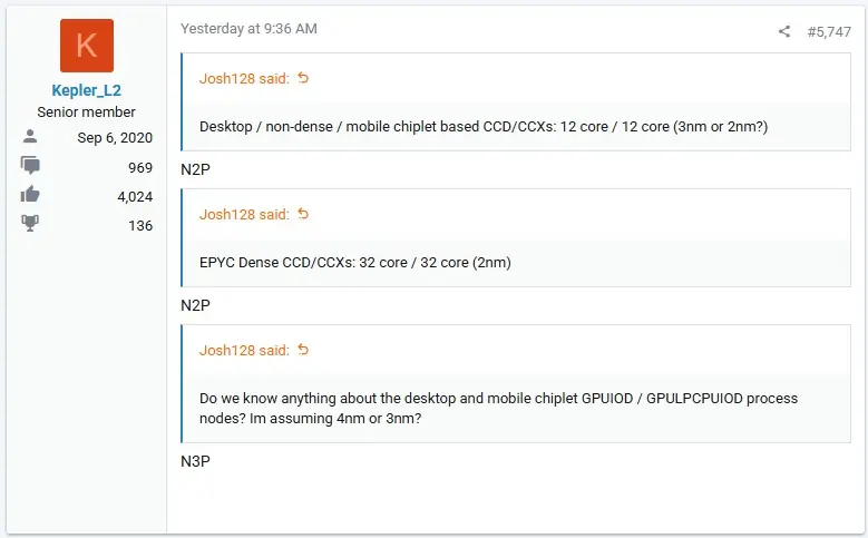
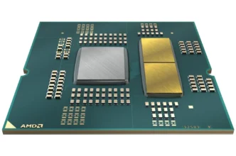
Furthermore, the use of TSMC’s 3nm N3P node for the I/O Die (IOD) represents another major upgrade from the current 6nm process. The IOD houses crucial components like memory controllers, PCIe interfaces, and integrated graphics.
Product Lineup and Core Counts
Leaks suggest that Zen 6 will feature increased core counts per CCD, with up to 12 cores and 24 threads, compared to Zen 5’s 8 cores. This, combined with an expanded L3 cache of up to 48MB per CCD, should translate to substantial performance gains, particularly in gaming.
The new architecture will power a range of products, including server EPYC processors codenamed “Venice,” desktop Ryzen CPUs under the “Olympic Ridge” codename, and high-end laptop processors like the “Gator Range.” For the mobile segment, the “Medusa Point” series will adopt a mixed approach, using N2P for CCDs and N3P for IODs in higher-end SKUs, while lower-end variants will be monolithic N3P designs. Other mobile platforms like “Medusa Halo” and “Bumblebee” are also anticipated.
Strategic Node Adoption
AMD’s decision to utilize TSMC’s performance-optimized ‘P’ series nodes (N2P and N3P) instead of the standard N2 and N3 nodes indicates a focus on maximizing performance. This multi-node strategy represents one of AMD’s most aggressive process node jumps, promising a significant generational uplift in CPU capabilities.
Via Kepler_L2