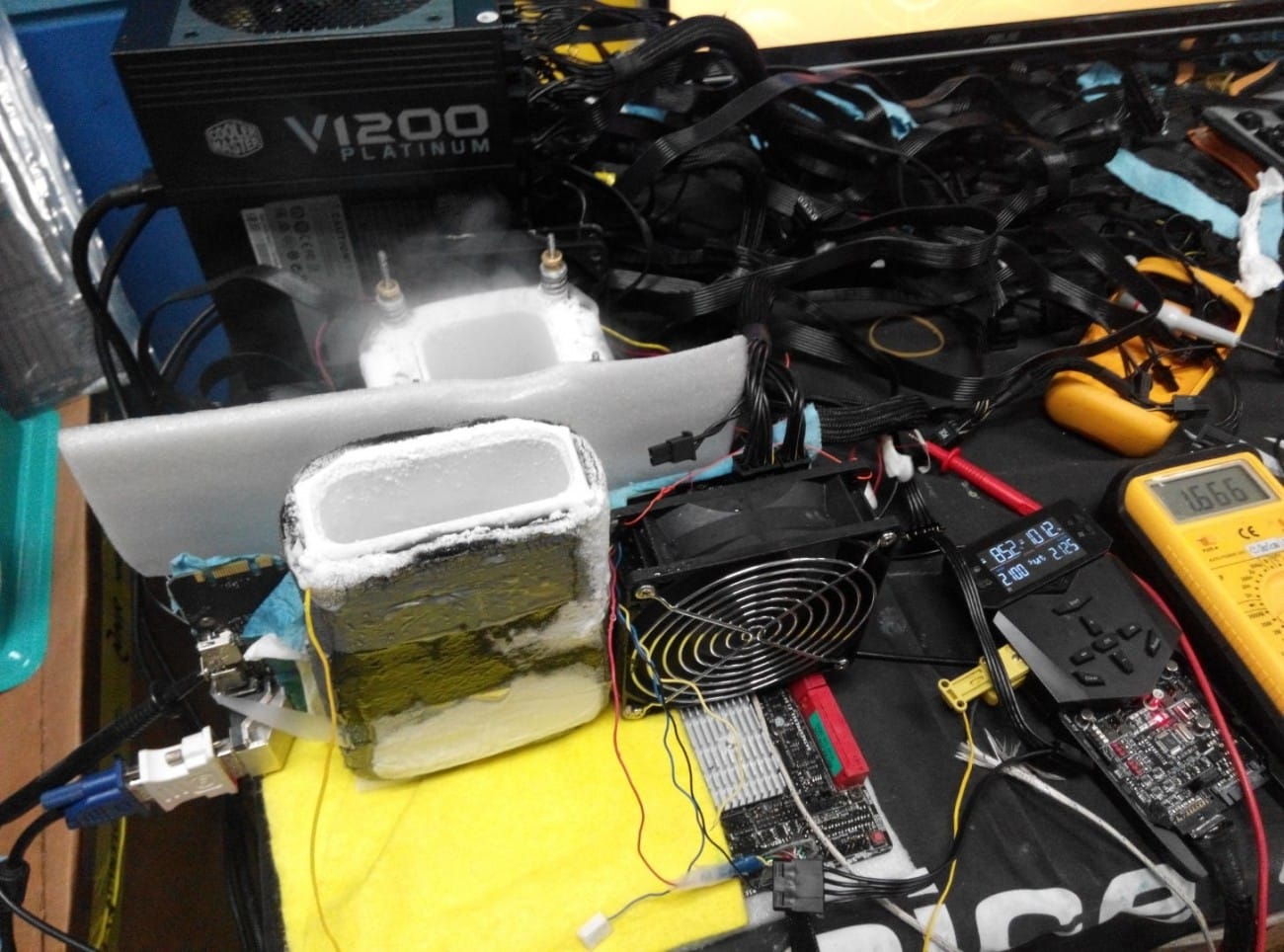
While we are all waiting for smaller fabrication nodes for GPUs, there is another revolution that will effect the graphics cards industry. High-Bandwidth Memory (HBM) is a form of stacked DRAM designed to sit on the same package as a processor. Hynix has been working on this technology with AMD and their entire HDM presentation was recently leaked giving us more insight on the technology.

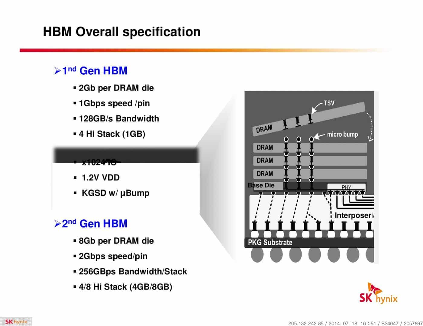
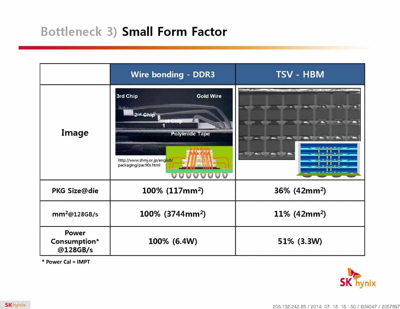
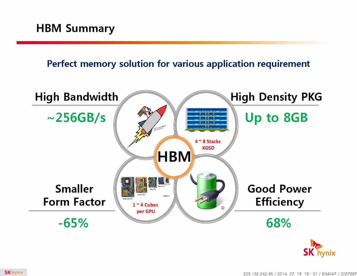
Hynix’s first generation High-Bandwidth memory will put four DRAM slices over a single base layer. These DRAM dies will be connected to each other with vertical channels called through-silicon vias (TSV). Each of these will be capable of transmitting 1 Gbps, which would give us 128 GB/s of bandwidth. First generation HBM will offer up to 4 dies per stack.
The second generation high-bandwidth memory is still being developed by Hynix. They are currently testing 256 MB slices forming 1 GB stacks. Soon they will be stacking 1 GB dies to form 4 GB modules. These are just 4-layer stacks. Further research and development will bring 8-layer stacks, which will be the only way to increase capacity (if I’m reading the slides correctly) as bandwidth will be to what 4-layers can offer. Second generation HBM will be available in 4 GB and 8GB stacks. The speed per stack will double to 256 GB/s.
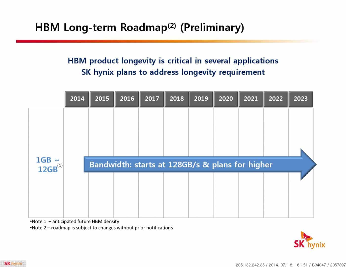
The above roadmap slide shows that late 2014 is the start so maybe we will see HBM on a new GPU, possibly Figi?
The entire presentation is below, click for larger images.


Source: Reddit via VideoCardz | News Archive