


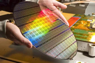
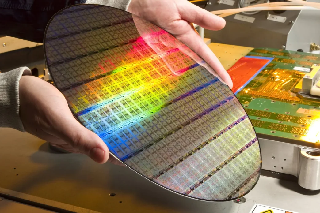
Tesla and SpaceX’s Terafab project is reportedly targeting capacity to process about 700,000 memory wafers per month by 2032—a scale comparable to estimates of Samsung’s current DRAM wafer capacity. The plan, disclosed to equipment suppliers according to Nikkei, would make memory the largest share of a proposed one-million-wafer monthly operation. It remains a long-term target, not current production.
Key takeaways
- Terafab reportedly plans capacity for 1 million wafers monthly by 2032: 700,000 for memory and at least 300,000 for logic.
- The memory target roughly matches estimates of Samsung’s present DRAM wafer capacity.
- Terafab is still in development; wafer capacity does not indicate how many finished chips it will produce.
For PC builders and hardware buyers, the announcement signals a possible future source of memory supply, but it offers no near-term change to component availability or pricing. The plan’s schedule, yields and intended memory products remain important unknowns.
A major memory-production target
The reported allocation puts roughly 70% of Terafab’s planned monthly wafer capacity toward memory. Samsung is estimated to process around 650,000 to 700,000 DRAM wafers per month, making the comparison striking—but not a direct measure of equivalent finished-product output. Terafab’s reported figure covers memory, and its precise product mix has not been disclosed.
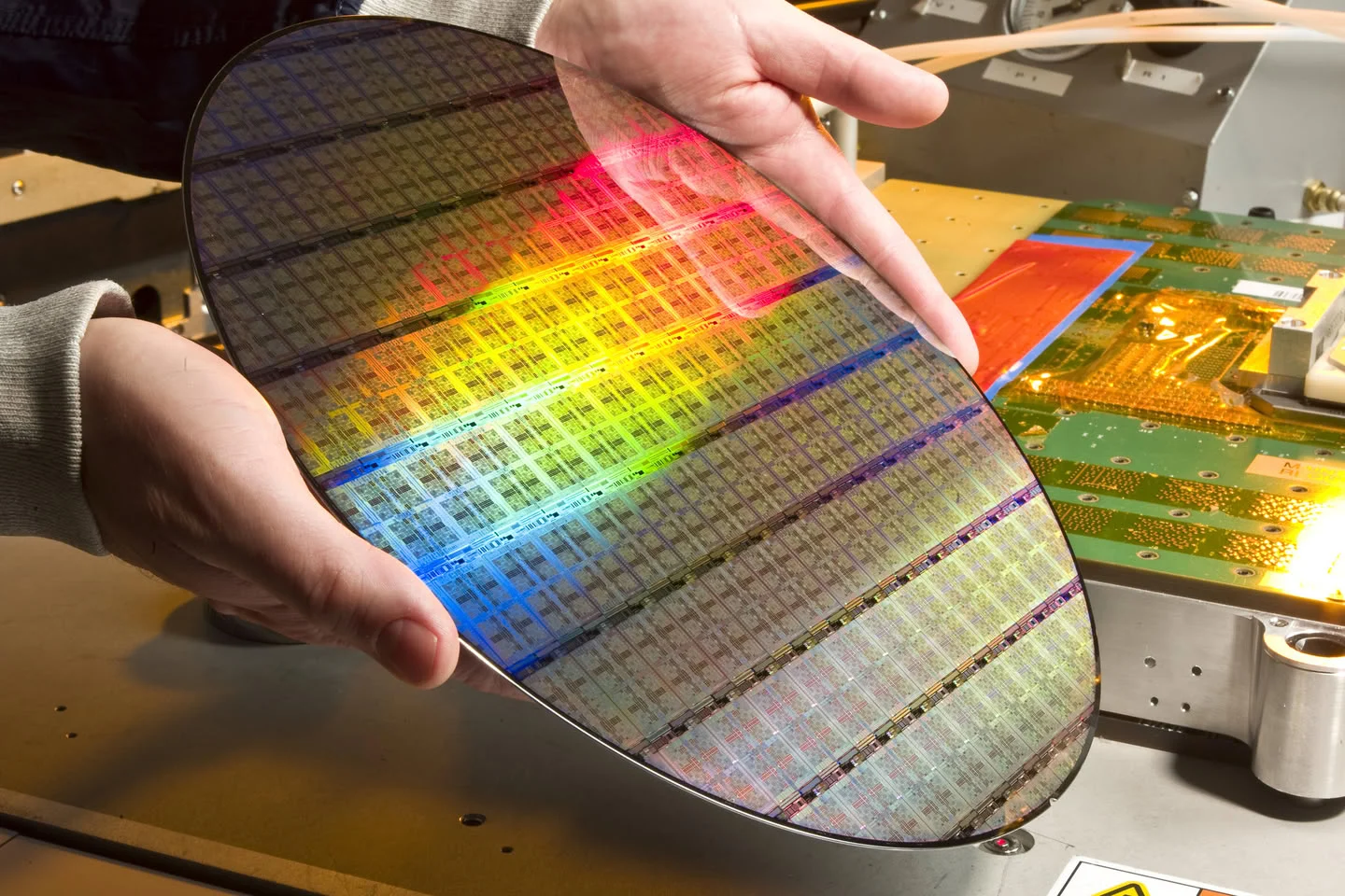
Terafab is a semiconductor venture backed by Tesla and SpaceX, intended to supply chips for uses including AI computing. The project aims to bring manufacturing steps such as logic and memory production, advanced packaging and testing together at a planned site in Grimes County, Texas. A first-phase investment of $16.8 billion has been announced, but that is not confirmation that the full expansion is funded or complete.
Capacity is not the same as supply
Wafer-processing capacity measures how many silicon wafers a facility can handle. Actual output depends on the memory type, manufacturing yields and subsequent packaging and testing. That distinction is especially relevant for advanced products such as high-bandwidth memory, whose assembly involves additional steps. Terafab has not confirmed that its target is specifically for DRAM or HBM.
The reported 2032 capacity goal is also separate from earlier development milestones. Elon Musk has said the project aims to run SRAM prototype chips at an Austin research fab in May or June 2027, with mass production at the main facility targeted for 2028. Those are ambitious targets, and reaching a prototype or beginning production would not mean the site had already achieved its long-term capacity.
What it could mean for PC hardware
If Terafab eventually produces memory at scale, it could help secure chip supplies for Tesla and SpaceX and potentially affect the wider market. But the companies have not disclosed how much output would be reserved for their own needs or sold to outside customers. Current memory supply and prices should not be expected to change on the strength of this target alone.
Terafab also reportedly intends to use Intel’s 14A process for logic chips, while discussions with TSMC over a possible partnership are said to be ongoing. The project’s eventual impact will depend on execution, product mix and usable output—not simply the headline wafer count.
Via WCCFTech