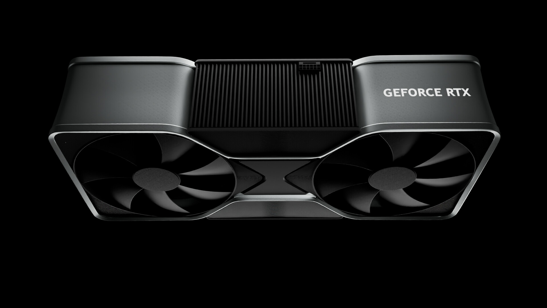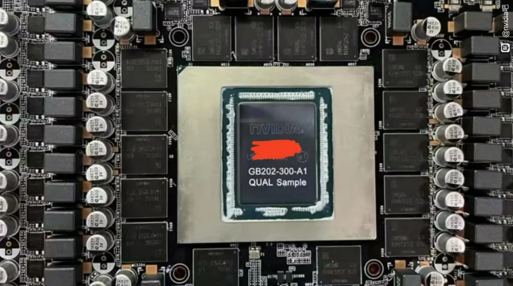
Here is what we believe to be the first photo of NVIDIA’s upcoming GeForce RTX 5090 “Blackwell” GPU. This follows up the earlier PCB leak and confirms what we saw there. What you see here is NVIDIA’s “GB202” silicon, which will power the GeForce RTX 5090 and will be the largest GPU based on the “Blackwell” graphics architecture. In the below photo we see that the silicon is labeled as “GB202-300-A1”. Since this is a “300” chip, not a “450” that we normally see on maxed-out NVIDIA ASICs, there is a possibility that the RTX 5090 might not have all streaming multiprocessors (SMs) enabled on the chip.

Surrounding the “GB202” chip are sixteen GDDR7 memory chips that will make up the expected 32GB memory on the card. The large pin count of the GPU, along with the memory chip count more or less confirm that this card will make use of a 512-bit wide memory bus. If the memory on the card is as expected at 28 Gbps we should see a memory bandwidth of 1792 GB/s! We can also see that surrounding the GPU and memory is a 24-phase VRM solution. Powering the card will be a single 16-pin 12V-2×6 power connector with NVIDIA likely maxing out the 600W power delivery there, so expect the card to have a TGP between 500-550W.
Via harukaze5719 (X)