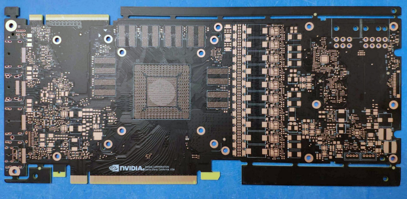
Here are some of the first photos of the bare printed circuit board (PCB) of NVIDIA’s upcoming GeForce GTX 1180 graphics card (being called PG180), and referred to by the person that leaked these photos as the “GTX 2080”, although most people are calling it the GTX 1180. This PCB looks to be right off the press as the SMT points and vias are still exposed. Looking at the traces the GT104 GPU should be about the same size as the GP104. The GPU is wired to eight memory chips on three sides, which confirms a 256-bit wide memory bus. Outputs looks to be flexible for either 2x DisplayPort + 2x HDMI, or 3x DisplayPort + 1x HDMI configurations.

The VRM setup is quite powerful as the card draws power from a combination of 8-pin and 6-pin PCI-Express power connections. There is a 10-phase VCore side, which is more than likely a 5-phase with “dumb” phase-doubling as well as a 2-phase for memory, which also could use phase-doubling (so 1-phase). We do spot a new connector which looks to be a single SLI finger and an NVLink finger arranged side-by-side.