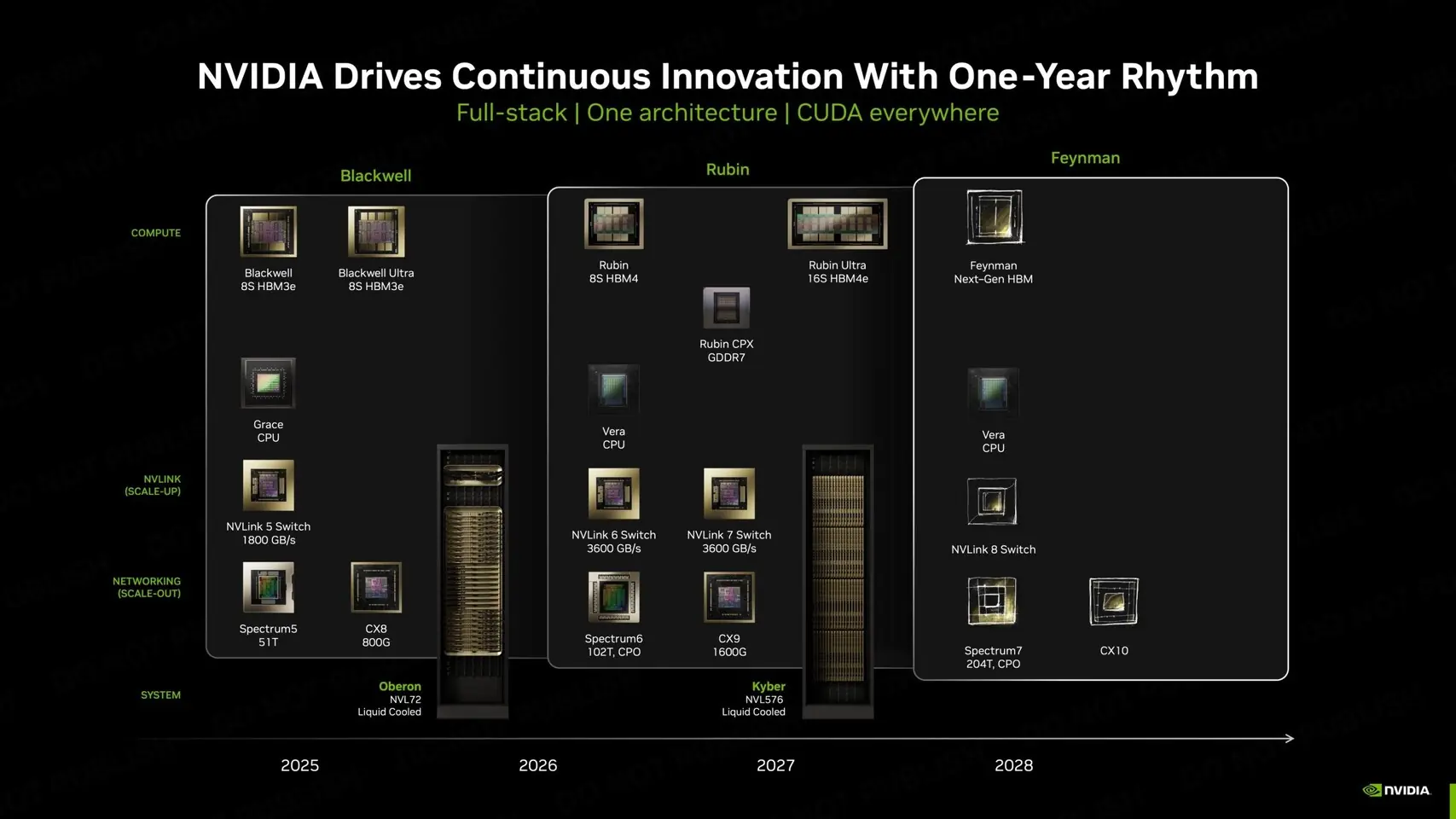
NVIDIA is reportedly set to leverage TSMC’s advanced A16 process node for its upcoming “Feynman” GPUs, expected to launch around 2028. This strategic move signifies a departure from Nvidia’s typical adoption patterns, as it aims to integrate TSMC’s most advanced technology, including backside power delivery, to maintain its performance leadership in the competitive AI and high-performance computing markets.
Key Takeaways
- Nvidia plans to utilize TSMC’s A16 process node for its “Feynman” GPU architecture.
- The A16 node is expected to enter mass production in the second half of 2026.
- This move marks Nvidia potentially being among the first to adopt TSMC’s A16, a 1.6nm-class node.
- The “Feynman” architecture is slated to succeed Nvidia’s “Rubin” series.
- The A16 node features backside power delivery and nanosheet transistors for improved performance and efficiency.
A Leap in Semiconductor Technology
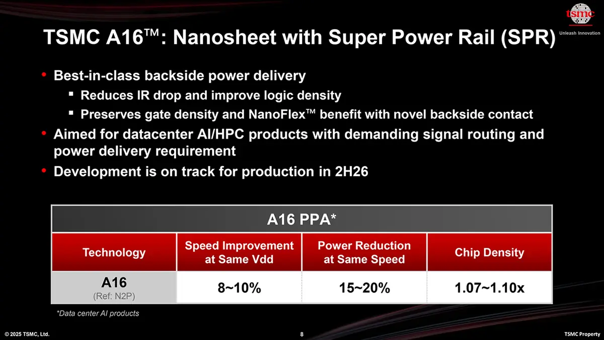
Nvidia’s “Feynman” GPUs are slated to be built on TSMC’s A16 process, a node that promises significant advancements. This 1.6nm-class technology is expected to incorporate features like backside power delivery and nanosheet transistors, aiming for enhanced chip density, improved performance, and reduced power consumption compared to previous nodes. The A16 node is anticipated to begin mass production in the latter half of 2026.
Strategic Shift and Competitive Landscape
This decision represents a notable shift for Nvidia, which has historically favored slightly more mature process nodes for its large-scale AI accelerators to ensure yield and thermal stability. However, with increasing competition, particularly from AMD, Nvidia appears poised to adopt TSMC’s leading-edge technology earlier than usual. The “Feynman” architecture is expected to follow Nvidia’s “Rubin” and “Rubin Ultra” GPUs, which are slated to use TSMC’s 3nm process.
Performance and Cost Considerations
TSMC’s A16 node is projected to offer an 8-10% performance improvement at the same voltage or a 15-20% power reduction while maintaining speeds comparable to the N2 (2nm) process. It also anticipates a 7-10% increase in chip density. While TSMC’s advanced nodes come at a premium, with reports suggesting costs exceeding $30,000 per wafer for Nvidia’s backside power delivery version, the substantial gains in performance and density are seen as justifying the investment for high-demand applications.
Future Implications
The adoption of the A16 node for “Feynman” could set a new precedent, with AI applications potentially leading the charge for TSMC’s most advanced process technologies, rather than consumer electronics like smartphones. The exact market segments for “Feynman” GPUs, whether AI/datacenter-focused or including broader consumer releases like GeForce RTX, remain to be seen.