


Samsung’s planned second semiconductor fab in Taylor, Texas, is reportedly already booked to its full expected capacity, with AMD accounting for most of the orders. The facility is slated to make advanced logic base dies for high-bandwidth memory (HBM), an increasingly important component in AI accelerators. Production is not expected to begin until 2030.
Key takeaways
- Samsung’s Taylor Fab 2 is reportedly fully booked, primarily for AMD, with NVIDIA also named as a customer.
- The roughly 2.7-million-square-foot facility is expected to use a 2nm process.
- Equipment installation is planned for 2029, ahead of mass production in 2030.
- Samsung has not confirmed customer details, and NVIDIA’s plans for HBM base dies remain uncertain.
Fab 2 targets HBM base dies
The reported plan centers on the logic die at the bottom of an HBM stack. This base die manages communication between the stacked memory and the processor; it is distinct from the DRAM layers themselves. Samsung reportedly intends to manufacture the logic dies in Texas and combine them with DRAM produced in South Korea to supply completed HBM products.
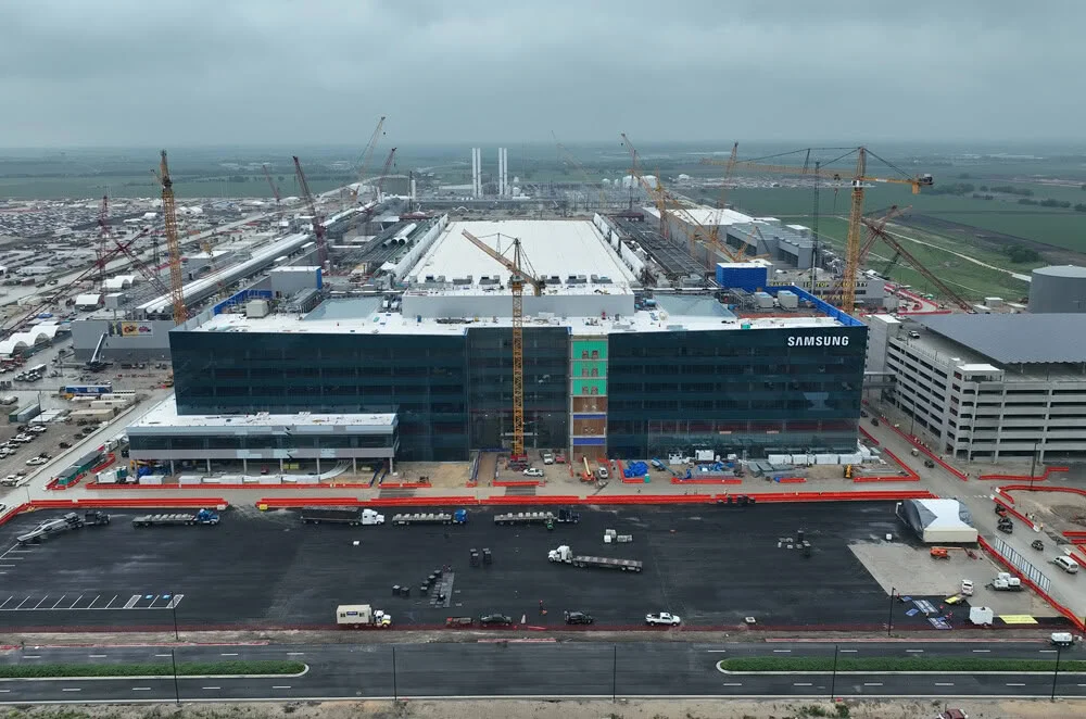
Samsung’s current mass-produced HBM4 and sampled HBM4E use 4nm base dies. The 2nm process planned for Taylor Fab 2 would instead target later HBM generations. That makes the project relevant to the broader AI hardware supply chain, rather than a direct production site for AMD CPUs or consumer graphics cards.
AMD is expected to take most of the capacity
South Korea’s Maeil Business Newspaper, cited in reports, says AMD’s orders make up the bulk of the fab’s planned output and could alone fill its capacity. The report follows Samsung’s selection as a preferred HBM4 supplier for AMD’s Instinct MI455X, announced in March, and comes as the companies explore wider foundry cooperation.
NVIDIA is also reportedly connected to the project, but its potential share is less clear. Reports say NVIDIA has asked memory suppliers to have base dies for its customized NVHBM produced by TSMC. If that strategy holds, it could limit Samsung’s opportunity to win additional NVIDIA orders. Traditional HBM and NVHBM may coexist during a transition, however.
Construction and production remain years away
Site preparation is underway, with formal construction expected to begin in November 2026. Equipment installation is projected to start in February 2029, followed by mass production in 2030. At about 2.7 million square feet, the fab is expected to be roughly 1.5 times the size of Samsung’s first Taylor facility.
The reported bookings would provide Samsung’s foundry business with a substantial prospective customer base, but they are not a guarantee of immediate output or profitability. Samsung declined to confirm customer-related details. For PC and gaming hardware watchers, the development is an upstream signal: competition for AI memory components is extending beyond DRAM to the advanced logic and packaging needed to connect memory with high-performance processors.
Via TrendForce