
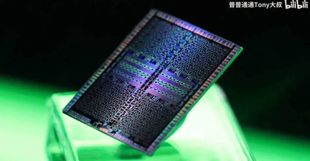
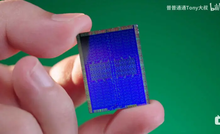
A die shot of NVIDIA’s GB202 has been revealed, which powers the RTX 5090. This impressive chip showcases the Blackwell architecture and is 24% larger than its predecessor, the AD102, featuring a staggering 24,756 cores and a 512-bit memory bus. The die shot not only highlights the GPU’s massive size but also provides insights into its intricate design and advanced technology.
Key Takeaways
- The GB202 die measures approximately 761 mm², making it 24% larger than the AD102.
- It features 24,756 CUDA cores, 192 RT Cores, and 768 Tensor Cores.
- The GPU utilizes a 512-bit memory bus and supports GDDR7 memory, enhancing bandwidth and efficiency.
- The die shot reveals a well-organized layout, with significant components like L2 cache and memory controllers strategically placed.
Overview of the GB202 Architecture
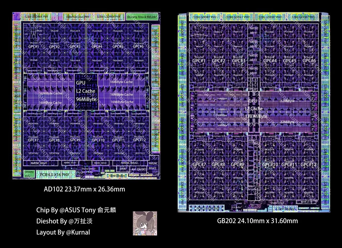
The GB202 die shot, shared by ASUS’s Tony Yu, showcases the layout of NVIDIA’s Blackwell architecture. The die is designed with a central L2 cache, surrounded by 12 graphics processing clusters (GPCs). Each GPC contains several texture processing clusters (TPCs), which house the streaming processors responsible for executing tasks.

The die’s layout is meticulously organized:
- L2 Cache: Located centrally, divided into multiple 2 MB chunks.
- Graphics Processing Clusters: 12 GPCs surrounding the L2 cache, each containing TPCs.
- Memory Controllers: Eight 64-bit memory controllers flanking the L2 cache.
- Video Encoders/Decoders: Positioned centrally for efficient video processing.
Size Comparison with Previous Generations
The GB202 is not only larger than the AD102 but also surpasses other previous NVIDIA architectures in terms of core count and memory bandwidth. Here’s a quick comparison:
| GPU Model | Die Size (mm²) | CUDA Cores | Memory Bus |
|---|---|---|---|
| GB202 | 761 | 24,756 | 512-bit |
| AD102 | 616 | 16,384 | 384-bit |
| GA102 | 628 | 10,496 | 320-bit |
| TU102 | 754 | 4,608 | 384-bit |
Technological Advancements
The GB202 leverages TSMC’s N4P process node, a refined version of the N4 node used in the Ada Lovelace architecture. This advancement allows for a higher transistor density, with the GB202 boasting approximately 92.2 billion transistors. The increase in die size and transistor count contributes to improved performance and efficiency, making it a formidable contender in the graphics card market.
Conclusion
The unveiling of the GB202 die shot marks a significant milestone in NVIDIA’s GPU development. With its impressive specifications and advanced architecture, the RTX 5090 is set to redefine gaming and graphics performance. As enthusiasts eagerly await its release, the GB202 stands as a testament to NVIDIA’s commitment to pushing the boundaries of technology in the graphics industry.
Via: ASUS China Tony Yu


