It has been over a month now since the GTC conference 2022 and finally, after all this long wait the pictures of NVIDIA’s latest data center GPU have been published by ServeTheHome.
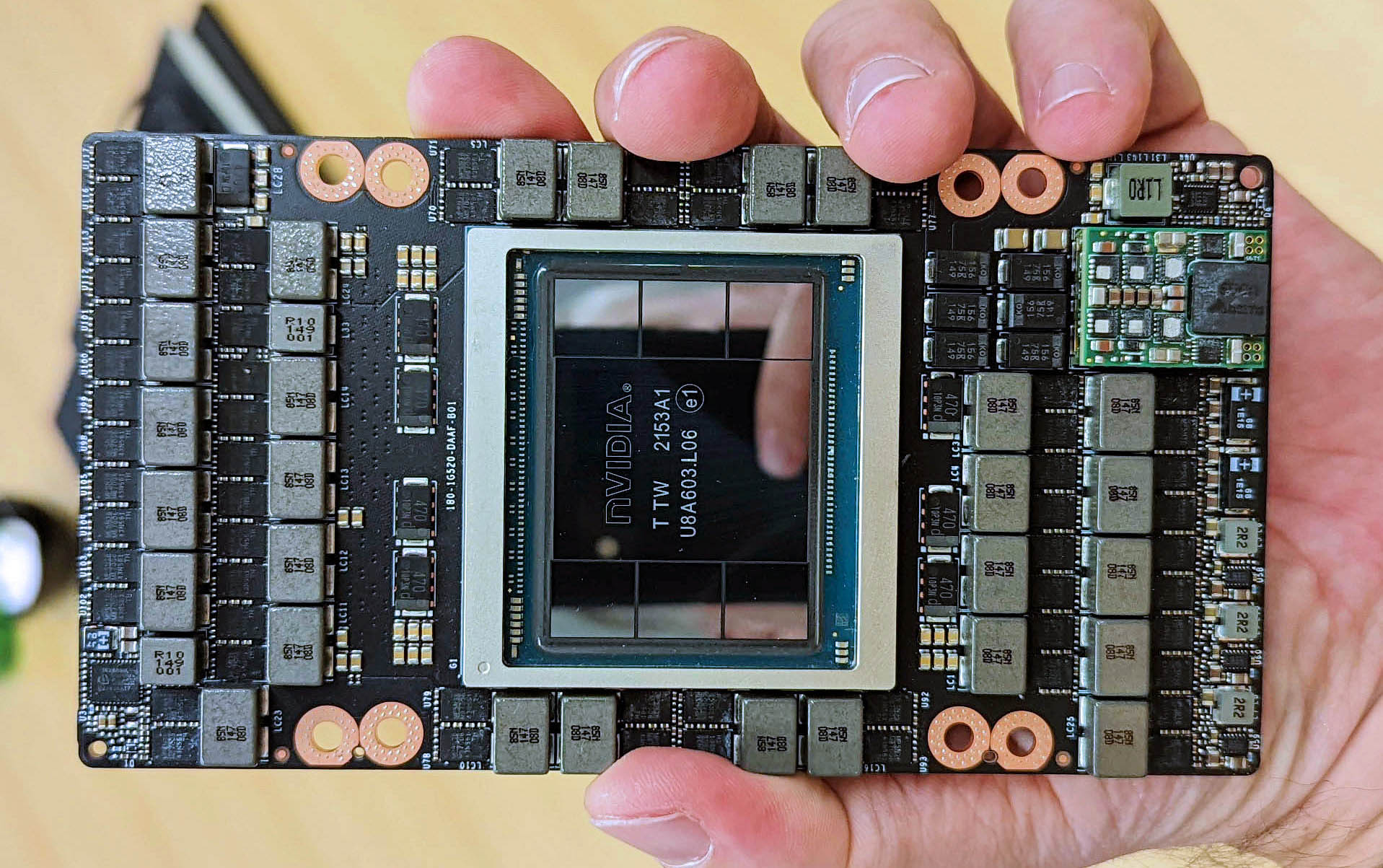
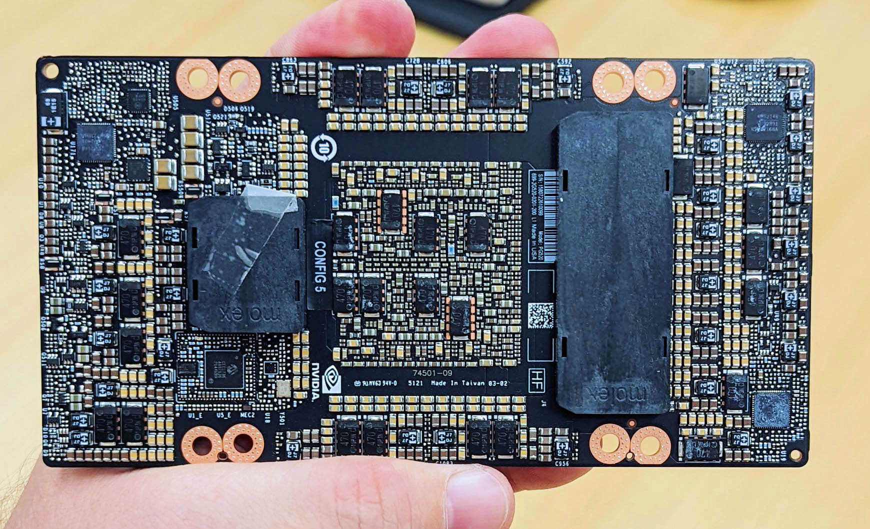
The H100 is the newest accelerator which comes with a 4 nm GPU build and is designed based on the Hopper architecture. Up until now, we had only been looking at various renders of this but now finally we get the new design on the SXM form factor in real pictures. ServeTheHome has also confirmed that the H100 will have a board featured called the PG520.

The NVIDIA H100 has made use of the TSMC CoWoS packing technology which makes use of a 814 mm² large GH100 GPU die along with six memory modules. This variant in particular has 16896 CUDA cores and will come with HBM3 memory of 80 GB. The SXM mezzanine connectors we see on this variant are different from what we saw on the A100. NVIDIA has ditched the design featuring two long connectors on each side of the GPU for one shorter connector.
The H100 is more power consuming than the previous SXM data center GPUs which were designed on different architectures. This one will consume up to 700W in power.
It is available for pre-order in Japan for $ 33,000.
Via ServetheHome, VideoCardz