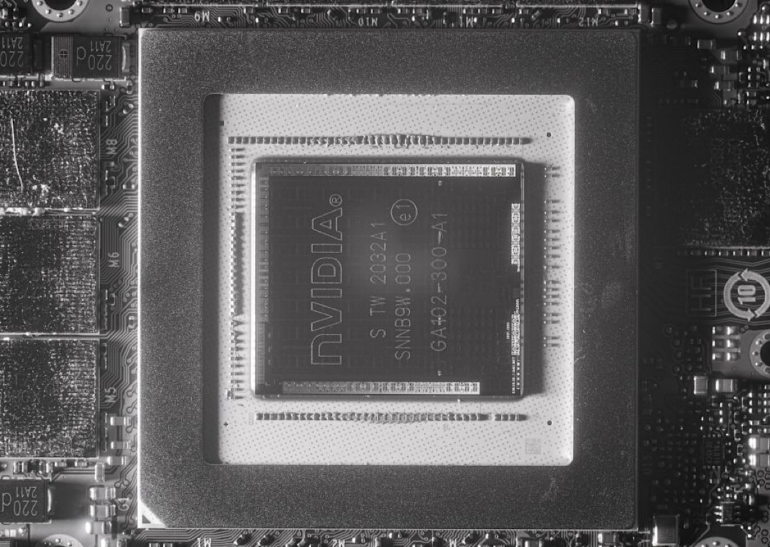
IR photography is the best way to get an in-depth look at silicon components, and a famous IR photographer Fritzchens Fritz has tweeted high-resolution photos of Nvidia’s GA102 Ampere silicon. This silicon is featured in GeForce RTX 3090 and RTX 3080, and it is rumored that the upcoming GeForce RTX 3080 Ti will feature it too.
The GA102 is the biggest mainstream Ampere gaming silicon created by NVIDIA. It features a 628.4 mm-squared die and is fabricated on the optimized version of the Samsung 8nm processor. The GA102 features 28.3 billion transistors along with the second-generation RT cores for ray tracing and third-generation Tensor cores for artificial intelligence workloads.
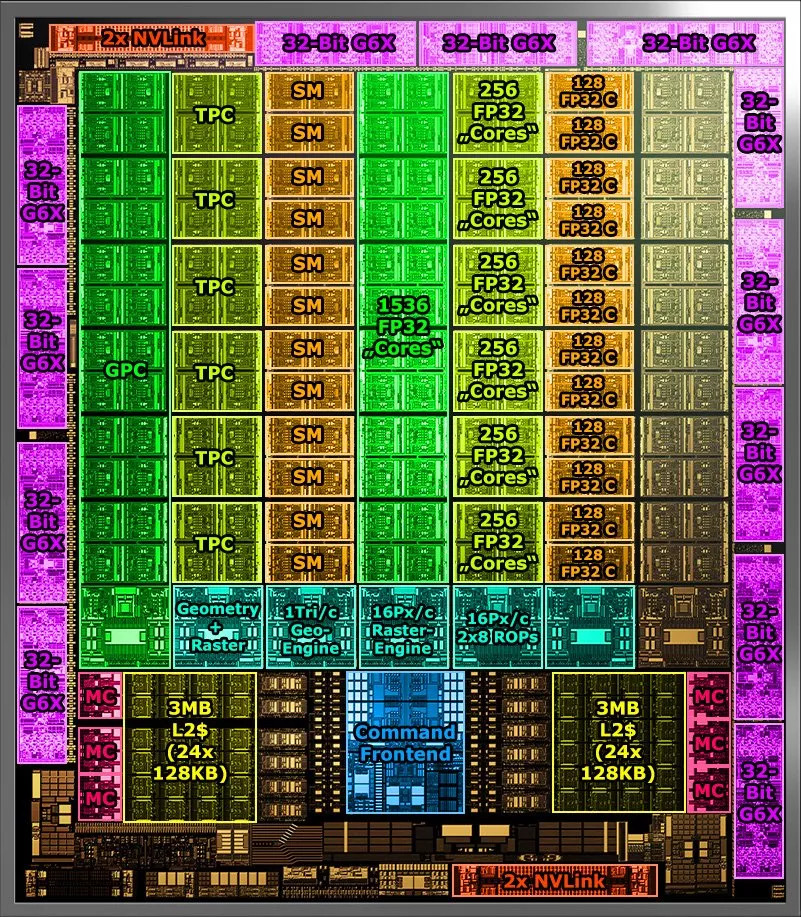
A Twitter user Locuza has added annotations to the photograph making it easier for you to visualize the technical specs. In case you don’t know about the specs, the GA102 features seven Graphics Processing Clusters (GPCs), and each GPC holds 12 Streaming Multiprocessors (SMs) thus the total count for SMs is 84. As for the specs for an individual SM, each SM features 128 CUDA cores, four Tensor cores, and one RT core. The total core count in the 84 SMs works out to be 336 Tensor cores, 10,752 CUDA cores, and 84 RT cores.
Via Twitter