Samsung claims the mass production of the industry’s smallest DRAM. It is based on extreme ultraviolet (EUV) technology which has a 14-nanometer process. In March( earlier this year), they started shipping the first EUV DRAM and it is going extremely well.
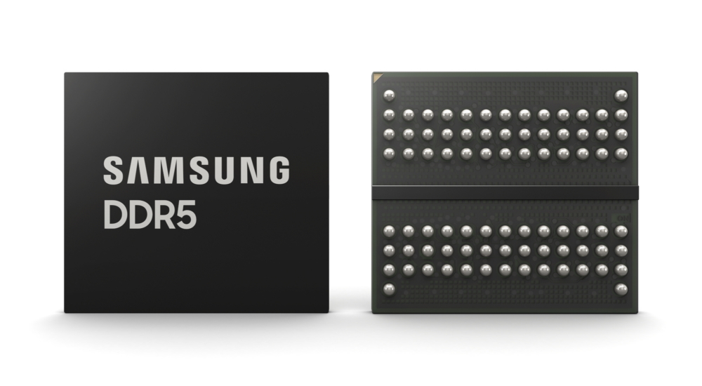
Samsung specifies that it has increased the number of EUV layers to five. They claim it is the most outstanding and most advanced DRAM process out there for the upcoming DDR5 memory solutions. It has given its entry at a time when Intel is ready to compete in the era of DDR5 in the customer landscape. Intel is introducing Alder Lake which will be accompanied by the Z690 platform.
According to Samsung, the EUV technology is increasingly significant as DRAM is going down the 10nm ladder. EUV gives the immense accuracy needed at this point, ensuring great performance and better yields. Samsung, with the use of five EUV layers on the 14nm DRAM was able to improve wafer productivity by 20 percent and decrease power consumption by almost 20 percent as well.
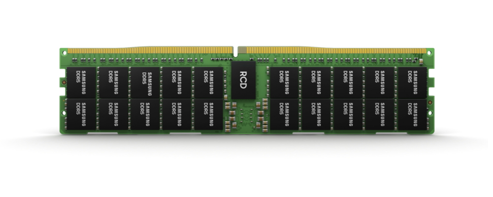
Samsung says the speed is 7.2 gigabits per second (7.2Gbps), double than that of DDR4, which works at 3.2Gbps. It also has chip densities of around 24Gb.
Samsung can now produce chips for use in 24GB, 48GB, 96GB, 192GB, and even 384GB DDR5-7200 memory solutions.
Via Samsung